Serial Peripheral Interface
 |
The Serial Peripheral Interface Bus or SPI (often pronounced "es-pē-ī" [IPA: ɛs pi aɪ] or "spy" [IPA: spaɪ]) bus is a synchronous serial data link standard named by Motorola that operates in full duplex mode. Devices communicate in master/slave mode where the master device initiates the data frame. Multiple slave devices are allowed with individual slave select (chip select) lines. Sometimes SPI is called a "four wire" serial bus, contrasting with three, two, and one wire serial busses.
Interface
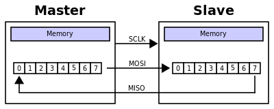
The SPI bus specifies four logic signals.
- SCLK — Serial Clock (output from master)
- MOSI/SIMO — Master Output, Slave Input (output from master)
- MISO/SOMI — Master Input, Slave Output (output from slave)
- SS — Slave Select (active low; output from master)
Alternative naming conventions are also widely used:
- SCK — Serial Clock (output from master)
- SDI, DI, SI — Serial Data In
- SDO, DO, SO — Serial Data Out
- nCS, CS, nSS, STE — Chip Select, Slave Transmit Enable (active low; output from master)
The SDI/SDO (DI/DO, SI/SO) convention requires that SDO on the master be connected to SDI on the slave, and vice-versa. That's confusing, so the MOSI/MISO convention is preferred.
- SPI port pin names for particular IC products may differ from those depicted in these illustrations.
Operation
The SPI bus can operate with a single master device and with one or more slave devices.
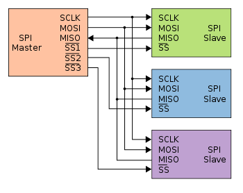
If a single slave device is used, the SS pin may be fixed to logic low if the slave permits it. Some slaves require the falling edge (high->low transition) of the slave select to initiate an action such as the MAX1242 by Maxim, an ADC, that starts conversion on said transition. With multiple slave devices, an independent SS signal is required from the master for each slave device.
Most devices have tri-state outputs that become high impedance ("disconnected") when the device is not selected. Devices without tristate outputs can't share SPI bus segments with other devices; only one such slave may talk to the master, and only its chipselect may be activated.
Data Transmission

To begin a communication, the master first configures the clock, using a frequency less than or equal to the maximum frequency the slave device supports. Such frequencies are commonly in the range of 1-70 MHz.
The master then pulls the slave select low for the desired chip. If a waiting period is required (such as for analog-to-digital conversion) then the master must wait for at least that period of time before starting to issue clock cycles.
During each SPI clock cycle, a full duplex data transmission occurs:
- the master sends a bit on the MOSI line; the slave reads it from that same line
- the slave sends a bit on the MISO line; the master reads it from that same line
Not all transmissions require all four of these operations to be meaningful but they do happen.
The transmissions normally involve two shift registers of some given word size, such as eight bits, one in the master and one in the slave; they are connected in a ring. Data is usually shifted out with the most significant bit first, while shifting a new least significant bit into the same register. After that register has been shifted out, the master and slave have exchanged register values. Then each device takes that value and does something with it, such as writing it to memory. If there is more data to exchange, the shift registers are loaded with new data and the process repeats.
Transmissions may involve any number of clock cycles. When there are no more data to be transmitted, the master stops toggling its clock. Normally, it then deselects the slave.
Transmissions often use single 8-bit bytes, and a master can initiate multiple such transmissions if it wishes/needs. However, other word sizes are also common, such as 16-bit words for touchscreen controllers or audio codecs, like the TSC2101 from Texas Instruments; or 12-bit words for many digital-to-analog or analog-to-digital converters.
Every slave on the bus that hasn't been activated using its slave select line must disregard the input clock and MOSI signals, and may not drive MISO. The master selects only one slave at a time.
Clock polarity and phase

In addition to setting the clock frequency, the master must also configure the clock polarity and phase with respect to the data. Freescale's SPI Block Guide [1] names these two options as CPOL and CPHA respectively, and most vendors have adopted that convention.
The timing diagram is shown to the right and described below:
- At CPOL=0 the base value of the clock is zero
- For CPHA=0, data are read on the clock's rising edge (low->high transition) and data are changed on a falling edge (high->low clock transition).
- For CPHA=1, data are read on the clock's falling edge and data are changed on a rising edge.
- At CPOL=1 the base value of the clock is one (inversion of CPOL=0)
- For CPHA=0, data are read on clock's falling edge and data are changed on a rising edge.
- For CPHA=1, data are read on clock's rising edge and data are changed on a falling edge.
That is, CPHA=0 means sample on the leading (first) clock edge, while CPHA=1 means sample on the trailing (second) clock edge, regardless of whether that clock edge is rising or falling. Note that with CPHA=0, the data must be stable for a half cycle before the first clock cycle. Also, that no matter what the CPOL and CPHA modes say, the initial clock value must be stable before the chip select line goes active.
This adds more flexibility to the communication channel between the master and slave.
Mode Numbers
The combinations of polarity and phases are often referred to as modes which are commonly numbered according to the following convention, with CPOL as the high order bit and CPHA as the low order bit:
| Mode | CPOL | CPHA |
|---|---|---|
| 0 | 0 | 0 |
| 1 | 0 | 1 |
| 2 | 1 | 0 |
| 3 | 1 | 1 |
Independent slave SPI configuration

In the independent slave configuration, there is an independent slave select line for each slave. This is the way SPI is normally used. Since the MISO pins of the slaves are connected together, they are required to be tri-state pins.
Daisy chain SPI configuration

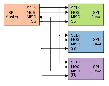
Some products with SPI bus are designed to be capable of being connected in a daisy chain configuration, the first slave output being connected to the second slave input, etc. The SPI port of each slave is designed to send out during the second group of clock pulses an exact copy of what it received during the first group of clock pulses. The whole chain acts as an SPI communication shift register; daisy chaining is often done with shift registers to provide a bank of inputs or outputs through SPI. Such a feature only requires a single SS line from the master, rather than a separate SS line for each slave.
This somewhat resembles SGPIO, although SGPIO is limited to particular backplane management activities and would not interoperate with most SPI chips.
Valid SPI communications
Some slave devices are designed to ignore any SPI communications in which the number of clock pulses is greater than specified. Others don't care, ignoring extra inputs and continuing to shift the same output bit. It is common for different devices to use SPI communications with different lengths, as, for example, when SPI is used to access the scan chain of a digital IC by issuing a command word of one size (perhaps 32 bits) and then getting a response of a different size (perhaps 153 bits, one for each pin in that scan chain).
Interrupts
SPI devices sometimes use another signal line to send an interrupt signal to a host CPU. Examples include pen-down interrupts from touchscreen sensors, thermal limit alerts from temperature sensors, alarms issued by real time clock chips, and headset jack insertions from the sound codec in a cell phone.
Pros and cons of SPI
Advantages
- Full duplex communication
- Higher throughput than I²C or SMBus
- Complete protocol flexibility for the bits transferred
- Not limited to 8-bit words
- Arbitrary choice of message size, content, and purpose
- Extremely simple hardware interfacing
- Typically lower power requirements than I²C or SMBus due to less circuitry (including pullups)
- No arbitration or associated failure modes
- Slaves use the master's clock, and don't need precision oscillators
- Transceivers are not needed
- Uses many fewer pins on IC packages, and wires in board layouts or connectors, than parallel interfaces
- At most one "unique" bus signal per device (chipselect); all others are shared
Disadvantages
- Requires more pins on IC packages than I²C, even in the "3-Wire" variant
- Lacks noise filtering of (fully compliant) I²C devices
- No in-band addressing; out-of-band chip select signals are required on shared busses
- No hardware flow control
- No slave acknowledgment (the master could be "talking" to nothing and not know it)
- Multi-master busses are rare and awkward, and are usually limited to a single slave
- Without a formal standard, validating conformance is not possible
- Only handles short distances compared to RS-232, RS-485, or CAN
Applications
The board real estate savings compared to a parallel I/O bus are significant, and have earned SPI a solid role in embedded systems. That's true for most System-on-a-chip processors, both with higher end 32-bit processors such as those using ARM and with lower end microcontrollers such as the AVR, PIC and MSP430. These chips usually include SPI controllers capable of running in either master or slave mode.
Chip or FPGA based designs sometimes use SPI to communicate between internal components; on-chip real estate can be as costly as its on-board cousin.
The full-duplex capability makes SPI very simple and efficient for single master/single slave applications. Some devices use the full-duplex mode to implement an efficient, high-speed data stream for applications such as digital audio, digital signal processing, or telecommunications channels, but most off-the-shelf chips stick to half-duplex request/response protocols.
SPI is used to talk to a variety of peripherals, such as:
- Sensors: temperature, pressure, ADC, touchscreens
- Control devices: audio codecs, digital potentiometers, DAC
- Communications: Ethernet, USB, USART, CAN, IEEE 802.15.4
- Memory: flash and EEPROM
- Real-time clocks
- LCD displays, sometimes even for managing image data
- Almost any MMC or SD card (SPI is an optional mode, widely supported)
For high performance systems, FPGAs sometimes use SPI to interface as a slave to a host, as a master to sensors, or for flash memory used to bootstrap if they are SRAM-based.
JTAG is essentially an application stack for SPI, using different signal names: TCK not SCK, TDI not MOSI, TDO not MISO, TMS not nCS. It defines a state machine, protocol messages, a core command set, the ability to daisy-chain devices in a "scan chain", and how vendors define new commands. Different vendors use different JTAG connectors. Bit strings used in JTAG are often long and not multiples of 8 bit words; for example, a boundary scan reports signal state on each of several hundred pins.
Standards
The SPI bus is a sort of de facto standard, rather than one agreed by any international committee. The reason for this is probably its essential simplicity.
However, that lack of standardization is reflected in a wide variety of protocol options. Different word sizes are common. Every device defines its own protocol, including whether or not it supports commands at all. Some devices are transmit-only; others are receive-only. Chip selects are sometimes active-high rather than active-low. Some protocols send the least significant bit first.
Some devices even have minor variances from the CPOL/CPHA modes described above. Sending data from slave to master may use the opposite clock edge as master to slave. Devices often require extra clock idle time before the first clock or after the last one, or between a command and its response. Some require an additional handshake signal to indicate when data are ready; that handshake doesn't always use MISO/MOSI signaling. Some devices have two clocks, one to "capture" or "display" data, and another to clock it into the device. Many of these "capture clocks" run from the SS line.
There are even hardware-level differences. Some chips combine MOSI and MISO into a single data line (SI/SO); this is sometimes called "3-Wire" signaling (in contrast to normal "4-wire" SPI). Anyone needing an external connector for SPI defines their own. Signal levels depend entirely on the chips involved.
Some devices provide an additional signal for flow control: the device must signal "ready" after a command is issued, before the host starts clocking in response data. (Most SPI masters don't support that signal directly, and instead rely on fixed delays.)
Related Terms
Queued Serial Peripheral Interface (QSPI)
The queued serial peripheral interface (QSPI) is one type of SPI controller, not another bus type. It uses a data queue with programmable queue pointers that allow some data transfers without CPU intervention[2]. It also has a wrap-around mode that allows continuous transfers to and from the queue with no CPU intervention. As a result, the peripherals appear to the CPU as memory-mapped parallel devices. This feature is useful in applications such as control of an A/D converter. Other programmable features in QSPI are chip selects and transfer length/delay.
SPI controllers from different vendors support different feature sets; such DMA queues are not uncommon, although they may be associated with separate DMA engines rather than the SPI controller itself. Most SPI master controllers integrate support for up to four chipselects, although some require chipselects to be managed separately through GPIO lines.
Microwire
Microwire is essentially a predecessor of SPI. It's a strict subset: half duplex, and using SPI mode 0. (Microwire-Plus supports other SPI modes.) Microwire chips tend to need slower clock rates than newer SPI versions; perhaps 2 MHz vs 20 MHz. Some Microwire chips also support a 3-Wire mode (see below), which fits neatly with the restriction to half duplex.
3-Wire Serial Busses
As mentioned above, one variant of SPI uses single bidirectional data line (Slave Out/Slave IN, called SISO) instead of two unidirectional ones (MOSI and MISO). Clearly, this variant is restricted to a half duplex mode. It tends to be used for lower performance parts, such as small EEPROMs used only during system startup and certain sensors, and Microwire. At this writing, few SPI master controllers support this mode; although it can often be easily bit-banged in software.
When someone says a part supports SPI or Microwire, you can normally assume that means the four-wire version.
However, when someone talks about a part supporting a 3-Wire serial bus you should always find out what they mean. They might mean standard four-wire SPI ... excluding the chipselect pin from that count, since most busses use chipselects but only three wires carry "real" signals. (Plus, sometimes with an unshared SPI bus segment the device's chipselect will be hard-wired as "always selected".) They might mean "real" 3-wire SPI. They might even mean an RS232 cable with just RXD, TXD, and shield/ground, or an application-specific signaling scheme.
References
- ^ SPI Block Guide V03.06, Freescale Semiconductor
- ^ Queued Serial Module Reference Manual, Freescale Semiconductor
See also
- I2C, sometimes called "2-wire" bus
- 1-Wire
- Microwire
- Computer bus
- Controller Area Network
- Serial communications
- Peripheral
- Interface
External links
- Introduction to Serial Peripheral Interface article on embedded.com
- Serial buses information page
- SPI Introduction with helpful diagrams
- Serial Flash Lots of good information on SPI part manufacturers and models.
