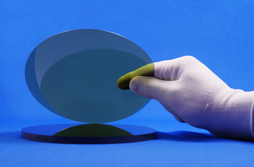
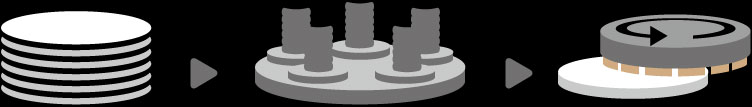
This is an ingot slicing method where a separation layer (KABRA layer) is formed at a specified depth by continuously irradiating an ingot with a laser, producing wafers starting from the KABRA layer.
In addition, this process can be applied to various types of SiC ingots, including single-crystal (4H, 6H, and semi-insulation) and multi-crystal ingots. This process can be also applied to monocrystal ingots, regardless of the off-angle of the crystal c-axis.
In addition, this process can be applied to various types of SiC ingots, including single-crystal (4H, 6H, and semi-insulation) and multi-crystal ingots. This process can be also applied to monocrystal ingots, regardless of the off-angle of the crystal c-axis.
- *1: Patented / Trademark registered


The existing methods for slicing wafers from a SiC ingot mostly used a diamond wire saw. However, these methods require a number of diamond wire saws for mass-producing wafers because the processing time is long due to the high hardness of SiC. The number of wafers produced from a single ingot is also small due to a large amount of material lost in the slicing sections. This has been a major factor in the increased cost of producing SiC power devices.


Processing time is
greatly reduced
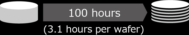
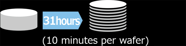
Existing processes require approx. 3.1 hours to slice a wafer from a Φ6-inch SiC ingot (100 hours for one ingot)*2, 3. In contrast, KABRA can greatly reduce the processing time, requiring only 10 minutes to slice a wafer (approx. 31 hours for one ingot)*4.
- *2: When producing a specified thickness of 350 µm from Φ6-inch and 20 mm thick SiC ingot.
- *3: General value based on users' information.
- *4: When laser irradiation, separation, and ingot grinding are performed in parallel using multiple ingots.
Existing process
KABRA process

Lapping process is
no longer required
For wire processing, a lapping process is required to remove approx. 40 µm*3 of undulations generated on the surface of a processed wafer. However, KABRA does not require lapping because the wafer undulation after separation can be controlled.
- *3: General value based on users' information.
Existing process
KABRA process

Number of wafers produced increases
1.4 times more than
that of existing processes
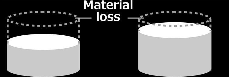
While wire processing produces approx. 180 μ m*3 of material loss per wafer where the ingot is sliced (kerf loss), KABRA has essentially no material loss. In addition, material loss can be suppressed to approx. 80 μ m depending on the amount of KABRA layer removal after separation. Thus, approx. 1.4 times as many wafers can be produced from a single ingot compared to the existing process.
- *3: General value based on users' information.
Existing process
KABRA process

Fully Automatic KABRA System
KABRA!zen®
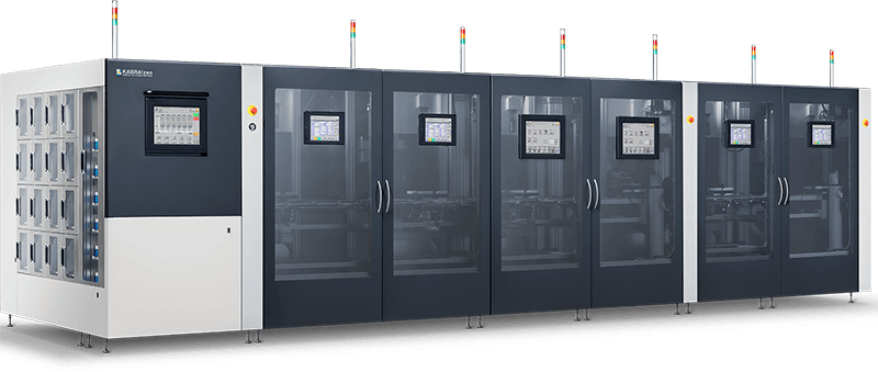

Φ8 inch ingot processing
Supports a maximum ingot thickness of 40 mm
- Machine dimensions (W×D×H):6,740×2,755×1,800 mm

“Kabra” is also another name for a turnip, and thin slicing is sometimes called “kabra-giri”. There is also a vegetable called “kyo-kabra” which is a traditional food with a long history in Japan. We named this process “KABRA” with Roman letters because slicing a SiC ingot looks like “kabra-giri” and we have the strong desire to contribute to enhancing the world’s convenience by spreading this unique laser slicing technique from Japan throughout the world.

No. of registered patents: 45 / No. of patent pending: 69
(As of October 2021)
(As of October 2021)